Molecular Beam Epitaxy (MBE)
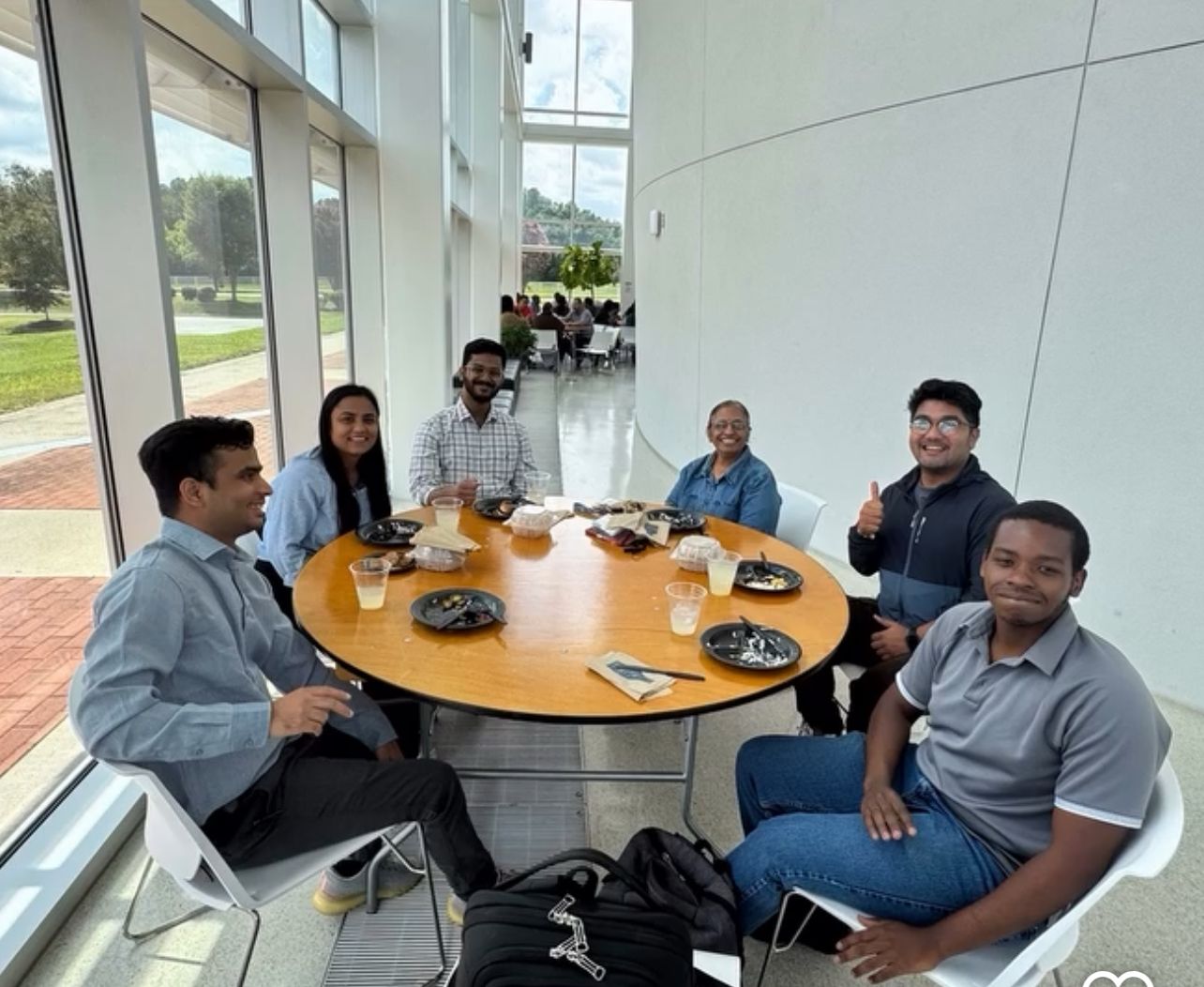
In molecular beam epitaxy (MBE), nanowires (and shorter “nanorod-like” 1D structures) are grown with atomic-level control, which lets researchers prec...
Read More
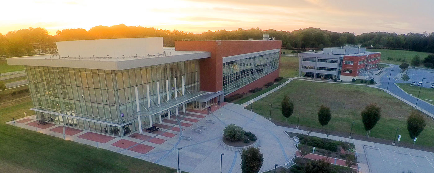

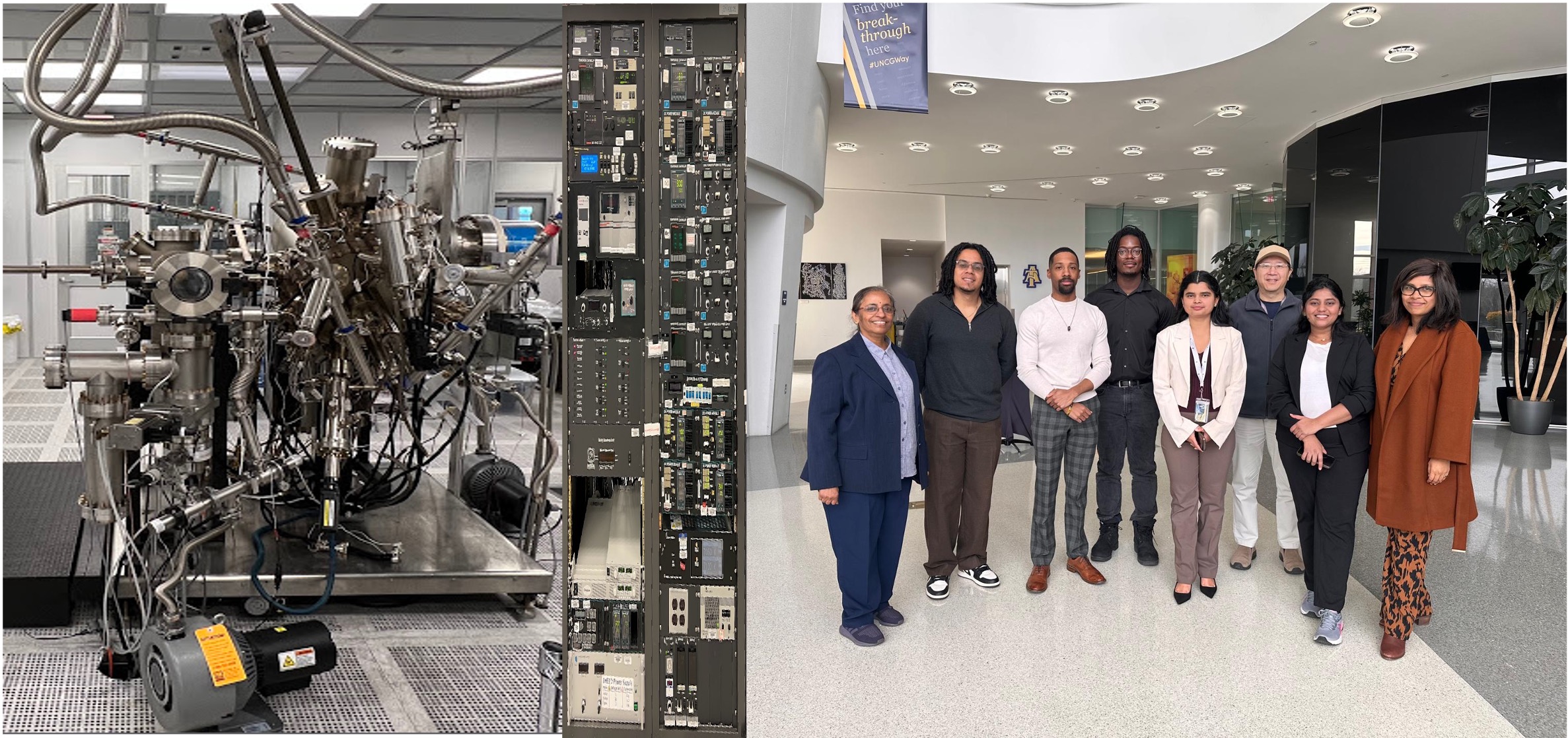
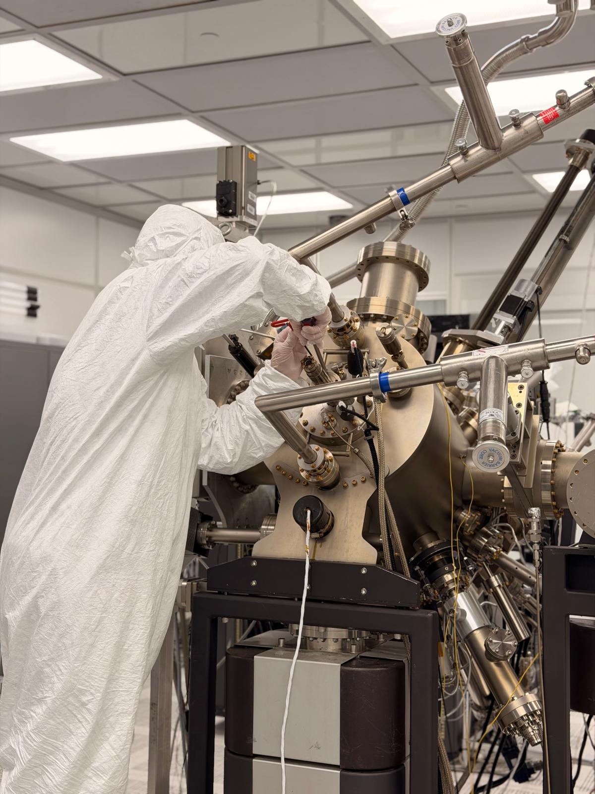
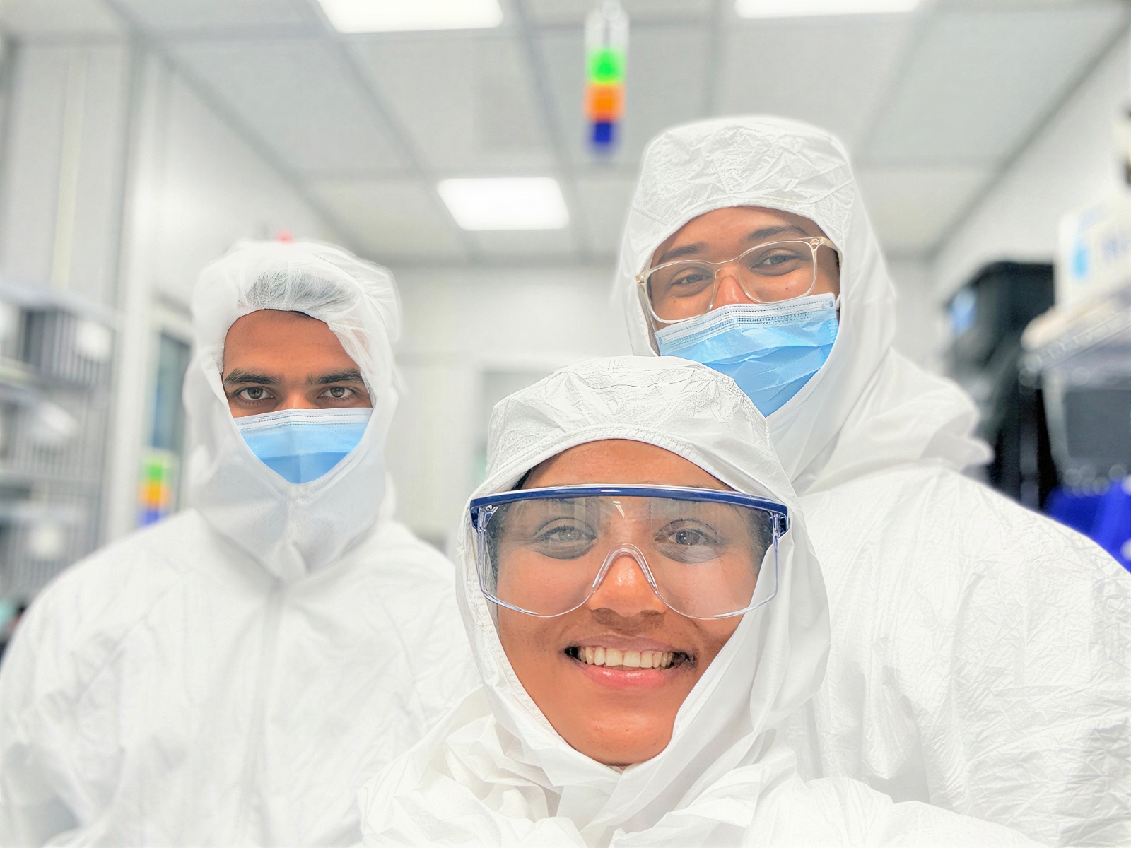
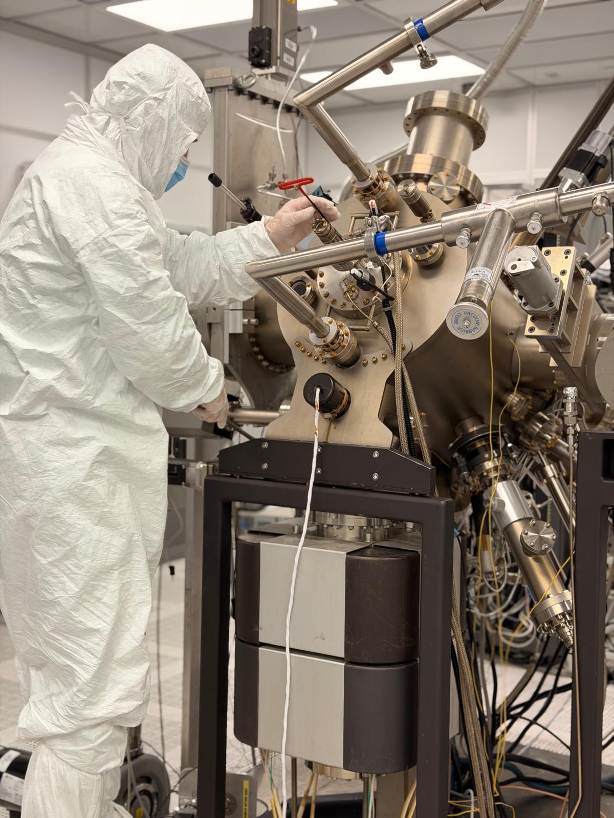
The Iyer Research Lab at the Joint School of Nanoscience and Nanoengineering (JSNN) focuses on designing and building advanced semiconductor nanostructuresespecially one-dimensional systems like nanowires using Molecular Beam Epitaxy (MBE). Our research combines materials growth, SWIR photonic sensors, multimodal characterization, and device fabrication to develop next-generation optoelectronic and photonic technologies.
Funding
Journal
Patents
Ph.D Students

Prof. Iyer initiated and developed NCA&TSU’s state-of-the-art Molecular Beam Epitaxy (MBE) Laboratory and associated academic and research programs. She has been a PI of over $10 million in DoD research projects. She was also the Director of the Center of Excellence for Battlefield Capability Enhancements, which focused on developing technologies for environmentally stable flexible panel displays. Her current research interests are molecular beam epitaxial (MBE) growth, SWIR photonic sensors, multimodal characterization, device fabrication, and fabrication of GaAsSb(N) nanowire-based infrared photodetectors epitaxially integrated into Si and graphene for next-generation photonic devices. This cross-disciplinary research encompasses solid-state physics, nanoengineering, and optoelectronic devices. Her group has carried out pioneering research in semiconductor nanowires, publishing over 32 journal papers and 3 patents in the past decade, focused exclusively on GaAsSb(N) nanowire growth, characterization, and high-performance photodetectors integrated on Si and graphitic substrates.
Know More About Advisor
Explore our latest research publications and academic works
ACS Applied Nano Materials,7 (21), 24299-24314 (2024)
Nanotechnology 35 (40), 405301 (2024)
Nanotechnology, 34, 265204 (10 pp) (2023).
Discover our latest research projects and findings
In molecular beam epitaxy (MBE), nanowires (and shorter “nanorod-like” 1D structures) are grown with atomic-level control, which lets researchers prec...
Read More

Greensboro, N.C. — At the Joint School of Nanoscience and Nanoengineering (JSNN), Prof. Shanthi Iyer is advancing a research program that sits at the...
Read MoreStay updated with our latest news and important notices
 Research Highlights
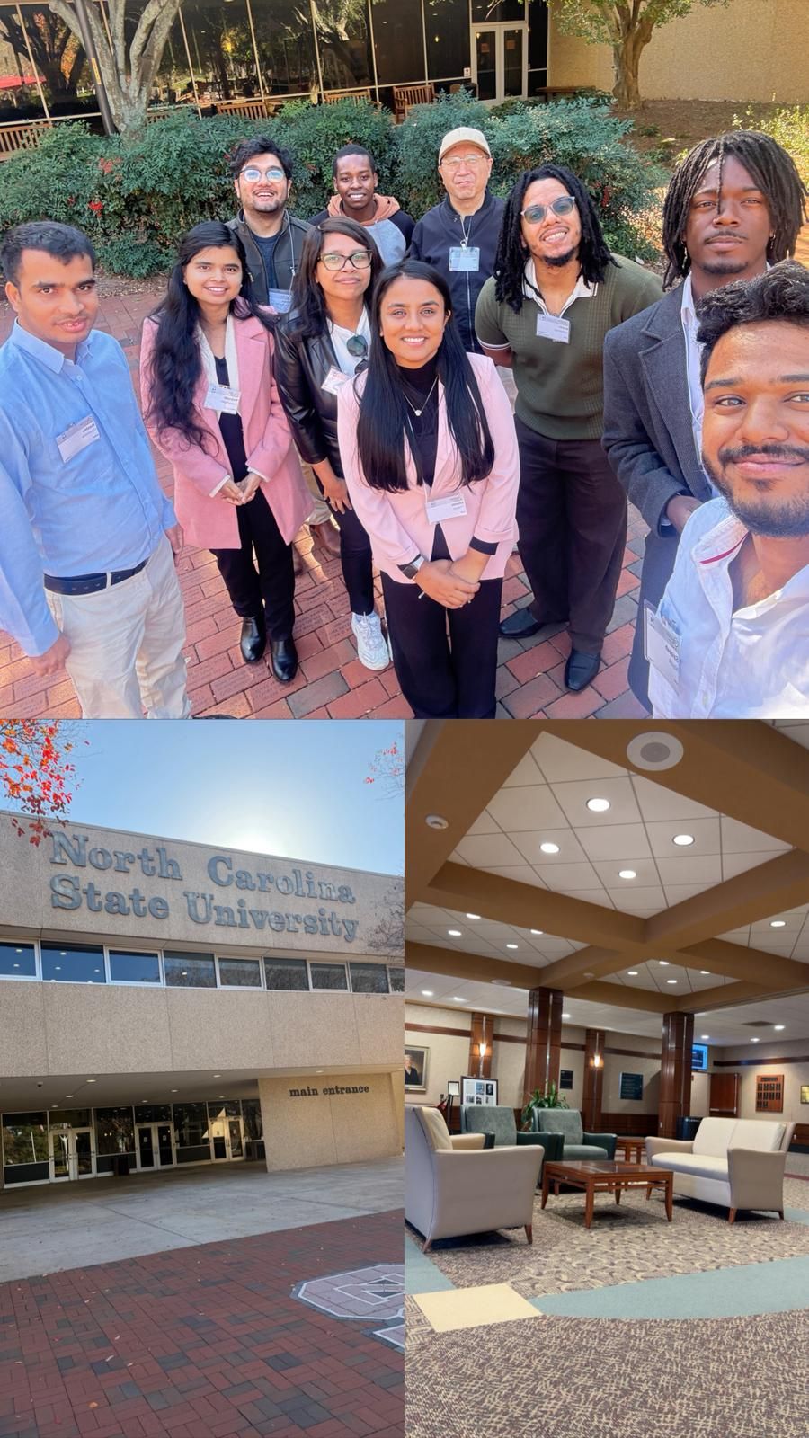 Conference Presentations
Browse through our latest photo collections